
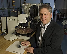
ALKHOBAR, 8 May 2007 — In nature a phenomenon called “self assembly” is a delicate process that forms seashells, creates the enamel on teeth and transforms water into snowflakes. IBM Research has, for the first time, applied “self assembly” to create a vacuum known as “airgaps,” the ultimate insulator, around nanowires for next-generation microprocessors. These computer chips are faster and smaller than ever before.
IBM has figured out how to control the self-assembly process to create trillions of tiny, nano-sized holes across a chip, which speed electrons that flow across wires inside the chip. In chips running in IBM labs using the technique, the researchers have proven that the electrical signals on the chips can flow 35 percent faster, or the chips can consume 15 percent less energy compared to the most advanced chips using conventional techniques.
These chips will go into our everyday electronics such as cell phones, computers and gaming consoles. The IBM patented self-assembly process moves a nanotechnology manufacturing method that had shown promise in laboratories into a commercial manufacturing environment for the first time, providing the equivalent of two generations of Moore’s Law wiring performance improvements in a single step, using conventional manufacturing techniques.
The self-assembly process already has been integrated with IBM’s manufacturing line in East Fishkill, New York, and is expected to be fully incorporated in IBM’s manufacturing lines and used in chips in 2009. The chips will be used in IBM’s server product lines and thereafter for chips IBM builds for other companies.
“This is the first time anyone has proven the ability to synthesize mass quantities of these self-assembled polymers and integrate them into an existing manufacturing process with great yield results,” said Dan Edelstein, IBM Fellow and chief scientist of the self-assembly airgap project. “By moving self assembly from the lab to the fab, we are able to make chips that are smaller, faster and consume less power than existing materials and design architectures allow.”
The importance of IBM’s breakthrough lies in the chip production. Today, chips are manufactured with copper wiring surrounded by an insulator, which involves using a mask to create circuit patterns by beaming light through the mask and later chemically removing the parts that are not needed. The new technique to make airgaps by self-assembly skips the masking and light-etching process. Instead IBM scientists discovered the right mix of compounds, which they pour onto a silicon wafer with the wired chip patterns, then bake it.
This patented process provides the perfect environment for the compounds to assemble in a directed manner, creating trillions of uniform, nano-scale holes across an entire 300 millimeter wafer. Once the holes are formed, the carbon silicate glass is removed, creating a vacuum between the wires — known as the airgap. The major difference in the IBM process is that while self-assembly processes that occur in nature are all unique, IBM has been able to direct the self-assembly process to form trillions of holes that are all similar.
HP has also made a major announcement in regards to commercially harnessing nanotechnology. The technology involves a process called nano-imprint lithography (NIL) — a method of literally stamping out patterns of wires less than 50 atoms wide on a substrate. HP Labs researchers have created patented NIL technology, which has enabled the fabrication of laboratory prototype circuits with wire widths of 15 nanometers — about one-third the dimension of the features in the most advanced circuits that will be commercially available this year.
Once the NIL “master” is created, copies can be stamped out quickly and inexpensively, like manufacturing CDs or phonograph records. The patterns are then filled in with metals for the wires. HP has licensed the technology to Nanolithosolutions, Inc., which has developed a tool that Bo Pi, CEO of Nanolithosolutions, stated will “enable reliable, repeatable processes for exploring biochips, photonics chips and many other applications.”
Stan Williams, HP Senior Fellow and Director, Quantum Science Research, HP Labs, believes that this new engineering development “will help create future generations of chips that will go beyond the capabilities of today’s fabrication technologies at an affordable cost.”